
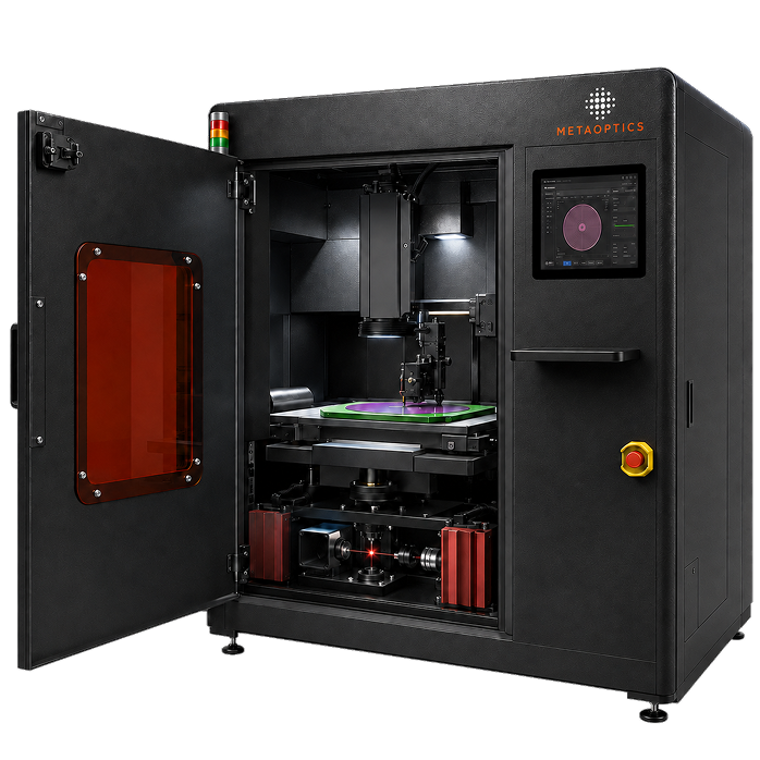
Built on a highly modular architecture, the manual testing platform prioritizes flexibility and scalability. It provides a practical starting point for precise metalens characterization that is designed to grow alongside your lab's evolving testing requirements.

Built for volume manufacturing lines.

Direct on-wafer characterization.

Shared modules across the tester line.

PSF, MTF, BFP and efficiency in one platform.

Tailored per application and sample.

R&D to Production
Direct on-wafer characterization of metalenses and metasurfaces, with per-die reporting:
A representative wafer-level production system, configurable per application:
Fiber-coupled, TEC-stabilized sources delivered to the illumination module via a single fiber output. Available variants:
Conditions the beam that reaches the wafer. Common kinematic interface — any of the following drops into the same slot:
Vacuum-clamped wafer chuck with air-cushion-assisted transport and per-die warpage compensation. Configurable for standard wafer sizes and coupon-scale samples:
Up to four independent stations populated around the objective. Available modules:
| Specification | VIS | NIR-I | NIR-II |
|---|---|---|---|
| Wavelength range | 400 – 700 nm | 700 – 1100 nm | 1100 – 1600 nm |
| Throughput | > 1000 UPH | ||
| Wafer compatibility | Up to 300 mm | ||
| Source options | Single LD, Switchable Multi-LD, Broadband + Filter | ||
| Total magnification | 20x – 150x | ||
| Supported focal lengths | Up to 5 mm | ||
| Angle of incidence | Up to 60° | ||
| Typical Z-step | 10 nm closed-loop piezo; 0.1 µm typical step in MTF / z-scan workflows | ||
| Maximum collected NA | 0.95 | ||
| Measurement modalities | MTF · PSF · BFP · Transmission · Fiber-Coupling Efficiency · WFE Estimation | ||
| Upgradeable measurement stations | Up to 4 | ||
Configurations / enhancements outside these ranges can be discussed on request.
The MetaOptics Wafer-Level Metalens Tester sits at the production end of a shared product line. The same source, illumination, and measurement modules run on the MetaOptics manual tester (R&D, prototyping) and the automated benchtop tester. A team that begins on the manual tester and ramps to wafer-level production carries its measurement methodology — and its modules — forward instead of starting from scratch.
Connect with us
Singapore (HQ)
Metaoptics Technologies Pte Ltd. 81 Ayer Rajah Crescent, #01-45 Singapore 139967
United States
Metaoptics Inc. (USA); 1 Ferry Building, Suite 201 San Francisco, CA 94111